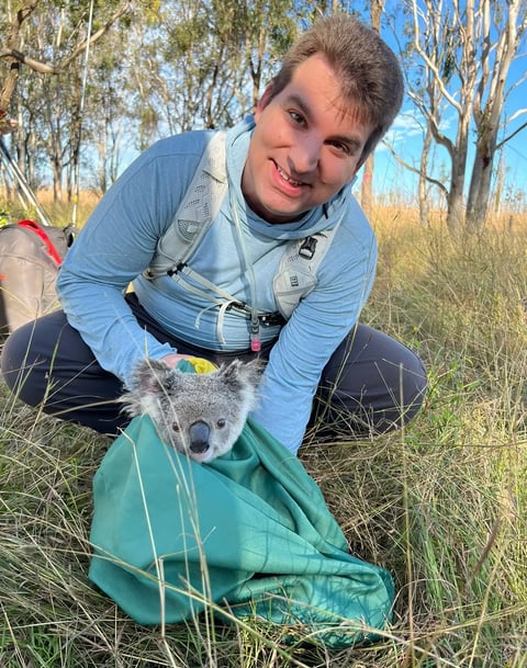
Office Hours: TBA (alternatively, you can e-mail me for an appointment)Syllabus: PDFTo make sure I get your e-mail, begin the subject with ECE327: or at least put 327 somewhere in the subject. An automatic filter will make sure your mail gets to me ASAP (rather than being marked as spam).
Most of the material will be covered. The final project, "Analog Pong Game," will be omitted due to lack of time.Schedule:
Week Date Topic 1 Mar 25 Lab 0: Introduction/Instrumentation 2 April 1 Lab 1: Bipolar Junction Transistor 3 April 8 Lab 2: Field Effect Transistor 4 April 15 Lab 3: Voltage Regulators 5 April 22 Lab 4: Oscillators 6 April 29 Lab 5: Analog-to-Digital Conversion 7 May 6 Lab 6: Digital-to-Analog Conversion 8 May 13 Lab 7 (1): Output Filtering 9 May 20 Lab 7 (2): Project Integration and Debugging 10 May 27 Report Due: Lab 7 (2): Project Integration and Debugging F June 5 Take-home final due at 11:59PM
Contents |
SOURCE CODE: I use LaTeX to generate the documents that I use for this class. I also export a public slice of my source control (i.e., docs but no tests) to the web so that you can view the source directly. Check out http://hg.tedpavlic.com/ece327/ to see the source "code" for the lab resources.
LICENSING AND REUSE: Unless otherwise expressly stated, all original material of whatever nature created by Theodore P. Pavlic and included in this website and any related pages, including its archives, is protected by copyright and licensed under a Creative Commons Attribution-Noncommercial 3.0 United States License ("CCPL"). Use of this website is expressly conditioned upon the user’s acceptance of the terms and provisions of the CCPL. Use of this site and any of the materials thereon constitutes acceptance of the CCPL by the user. Students enrolled in ECE 327 may reuse or modify portions of the materials without attributing the content to its original author so long as it is being used to generate a submission to the original author (e.g., the use of a schematic on a lab report to be submitted to T. Pavlic); otherwise, this web page URL, the URL of the source document, or the author’s name can be cited as the source of the work.
COMPONENTS: You may use the inventory of available laboratory resistors and capacitors to help you do any pre-lab calculations.
Over the quarter, I will collect tips from our daily lab experience and post them here.
Make sure your function generator is calibrated for high output impedance load. Look for a HIGH Z [1, 2] mode in the output settings (also called output termination). After changing this setting, go back to your waveform settings and enter the correct amplitude.
- Recall from your electromagnetics classes (e.g., ECE 311/312) that transmission lines must be terminated to prevent reflections. Conventional terminating loads are 50 ohms, which means that a function generator on one of these lines must drive a 50 ohm load. So, the function generator designers have embedded a 50 ohm load as the output impedance of the scope and purposely deliver twice the desired amplitude. When connected to a 50 ohm load, the resulting voltage divider provides the right amplitude because it has a gain of 0.5.
- In our class, load impedances (e.g., inputs to amplifiers) are much higher, and so the resulting voltage divider with the 50 ohm output impedance has near unity gain. Telling the function generator about our "HIGH Z" load prevents it from doubling the output.
- NOTE: When you change to "HIGH Z" mode, the function generator will change your output setting to twice its original amplitude. You will need to readjust it.
- Keep in mind that there is always a voltage divider at the output of the function generator, and so it is always best to use your digital multimeter (DMM) or your oscilloscope to tweak the function generator’s output.
Use a 10x (or x10 or 10:1) probe to increase the high-frequency impedance seen by the device under test (DUT).
- The capacitance of a standard 1x (or 1:1) probe creates a low-pass filter. A 10x probe adds series capacitance and resistance to compensate for this effect.
- The extra resistance of the probe is almost exactly 9x the input resistance of the scope, and so the signal on the scope is scaled by a tenth. Use the scope’s probe settings to automatically scale it to fix this.
The probe may need to be compensated. Please do not attempt this task yourself on the lab probes. However, recognize how it is done and file it away in your long-term memory for the next time you see ringing on a scope.
Most of our 10:1 probes have a small spring-loaded sense pin at their oscilloscope connection. When this pin or the scope connectors get dirty, it becomes difficult for the scope’s auto-detection features to work. Placing a small piece of paper between this pin and the scope should prevent the scope from trying to automatically change the probe settings. Cleaning these contacts may improve the situation.
Of course, the DMM may need a new battery; however, it’s usually the case that the DMM is in a cautionary mode to prevent it from being accidentally turned on.
While the DMM dial is turned to something other than "Off," press the two buttons under the display simultaneously. The DMM should "wake up" and be operable again.
To prevent the DMM from entering this mode, be sure to turn it off when you’re not using it. If the DMM is left on for a few subsequent long periods of time without much use, it will enter this sleep mode.
Use a bypass capacitor across your power rails and possibly near your circuit elements.
- Choosing the size and type of each of these can be complicated.
- A good rule of thumb is to put pretty large capacitors (e.g., multiple microFarads) at the central power rails and slightly smaller (e.g., 0.001–0.1 microfarads) on the power pins at each component.
Stray parasitic capacitance is everywhere. In fact, the pins of an IC and the air between them form a capacitor of at least a few picoFarad. If you can, try to choose circuit elements that dominate over or compensate for these strays.
If setting an RC, choose a low R to give you a high C; however, realize that the low R may result in a higher power draw from your circuit.
The Agilent oscilloscopes have an internal TRC ("Trace?") file format that are not easy to open on anything but the scopes themselves. Using the "Quick Print" button or being sure to check the "Formats" menu after clicking "Save" will let you save to more conventional formats like CSV and BMP.
If you have a bunch of TRC files, e-mail me to setup a time to visit the lab. You’ll be able to use the scope to open the TRC files on your disk and then re-save them as the format you like.
While it’s fine to include BMP ("BiTmaP") files in your lab report, CSV ("Comma Separated Values") files are much more versatile. Rather than storing an image, they store actual data that can be opened by Microsoft Excel or MATLAB (see the csvread command for one example of how to do this; try typing help csvread inside MATLAB). You’ll then be able to plot and manipulate the data as you wish.
When choosing resistor and capacitor values for your oscillator (e.g., when designing relaxation oscillators with a 555 timer IC), remember to dominate the stray parasitic resistances and capacitances present all over your breadboard.
Assume that the breadboard and chip pins contribute a few Ohms (even as many as ten or twenty) of resistance and a few picoFarads of capacitance to your circuit. Because of this, keep your resistances greater than a kiloOhm and your capacitances greater than 10 nanoFarad. Resistances lower than this are bad for your circuit anyway because they probably mean your burning too much power off.
Keep in mind that the above is just a rule of thumb. There are plenty of applications where large resistances (e.g., in the feedback path of operational amplifiers) are very bad things and will affect the bandwidth and stability of your circuits. Just try to anticipate the parasitics and work around them.
Your breadboard came with screw terminals for a reason. Banana plug connectors can plug into the terminals. Thus, setup your power rails by running wires from the three or four banana terminals on your board. When you’re ready, plug your power supply into the banana connectors directly. It’s much more convenient.
Unfortunately, many students throw away their banana connectors rather than attaching them. In the future, assemble your breadboards completely; they work better that way.
On the other hand, die-hard high-frequency analog prototypers will abandon breadboard use entirely for setting up "dead-bug" circuits on a bare copper ground plane. This practice, which places chips upside down making them look like dead bugs, can improve performance but is less flexible (it can require glue in some cases, and will definitely require solder). In our lab, using big enough bypass capacitors (see "Power supply noise" tip above) is the closest we’ll get to low noise prototyping.
Potentiometers are often used as two-terminal devices in this laboratory as variable resistors. Instead, try using all three terminals. A potentiometer is nothing more than a voltage divider, and the screw moves the output of the voltage divider (the middle pin) from the high voltage to the low voltage. If you need to tune a voltage divider, just use a potentiometer instead!
Keep in mind that you should probably choose a potentiometer with a size that only draws a few milliamps at most from your circuit. Even though you probably only care about the resistance ratios, you should care about the current draw (and power dissipation) as well. If not for any other reason, it will keep you from getting blisters when you touch your circuit.
There is no DC feedback through a capacitive feedback path. Additionally, every real OA has a small imbalance between its inputs that manifests itself like a small DC source connected to one of the inputs. So, the integrator integrates this small offset and produces an additional ramp on the output. In other words, the infinite DC impedance of the capacitor looks like an infinite DC gain at the output, so the OA tries to make its output have an infinite DC component after transients die out (i.e., the OA output goes to one of its rails).
One solution to this problem is to provide finite DC feedback with a large resistor (e.g., 1–10 megaOhm) in parallel with the feedback capacitor (i.e., the "Miller integrator"). Now, the small offset potential at the OA input will show itself as an amplified, yet hopefully still small, offset in the output. To reduce the amplification, the feedback resistor can be reduced. However, the smaller the feedback resistor, the greater the corner frequency of the lowpass filter you’ve just created. In other words, your circuit will look less like an integrator and more like a smoothing filter; low frequency signals will not be integrated well.
(note that some OA’s already have a large feedback resistance built into the device in order to ensure DC feedback. Capacitive leakage may also play a role. If you are noticing offset on your output rather than railing, it is most likely because there is an internal (or parasitic) large resistance in parallel with your capacitor)
Another solution is to capacitively couple your input to the integrator (i.e., place a LARGE capacitor (e.g., 1 microFarad or higher, which is probably only available polarized) in series between your signal and the integrator input). This method shifts your input signal by the offset potential, so the offset does not generate any additional current into the capacitor. Therefore, the offset will still be present at the output, but it will not be amplified.
If you are using the integrator as a ramp generator, neither of these solutions will work. Because you are probably feeding a constant (i.e., DC) signal to the input of the integrator, you would not want to amplify DC nor capacitively couple your input. Therefore, your only solution is to put the OA back into balance. The most general balancing method is to use the inverting input as a sum junction. Tie the outer legs of a potentiometer (e.g., a 10 kiloOhm) to your positive and negative rails. Tie the inner "wiper" to the inverting input of the OA. With the input of your integrator tied to 0 (or shorted to the non-inverting input of the OA), tune the potentiometer until the output is zero.
Most OA’s have "balance" pins that can be used to null the offset in a similar fashion. The usual procedure again involves a potentiometer. Tie the outer legs of the pot to the two balance pins, and tie the wiper to the negative rail. Short the inputs of the OA together, and adjust the pot wiper until zero appears on the output.
Keep in mind that OA offset varies with temperature and can drift with time. One of the reasons why electronics are "burned in" at the factory is to reduce the rate of drift (here, I have voltage references in mind). Therefore, nulling offset is a much more complicated problem in a product that has a lifetime longer than one class time. In our case, if we’re not using the integrator for a ramp generator, we should probably null the offset and do one of the other methods (i.e., capacitively couple the input signal or add a large feedback resistor).
Make sure that you didn’t swap your collector and emitter (i.e., make sure you don’t have your transistor plugged in backwards).
Take a look at the "Arrangement of n-Doped and p-Doped Regions" in Figure 1.2 of the lab text. As you can see, the only difference between the emitter and the collector are the "size." The base-emitter diode is "small" and the base-collector diode is "large." As a consequence, a transistor "works" when emitter and collector are reversed, but the current gain will be very low (e.g., the collector current might be equal to the base current). Our models of a transistor assume that the current gain is relatively infinite, and so they will poorly predict how a circuit will work in the other case.
Because of the "size" of the base-emitter diode, it is easy to reach the reverse breakdown voltage of the base-emitter diode if it is connected improperly. So, hooking a transistor up "backwards" can either damage the transistor or simply produce a poorly performing circuit.
Great reference for advanced students. Classic electronics reference. Highly respected. The [analog] electronics bible.
Standard microelectronics text. More focus on younger undergraduate student audience. Lots of details, but very little breadth. Poor reference for advanced students. In fact, so many details are given that the text can be a poor reference for novices as well.
This website presents lengthy discussions of circuits for beginners. The discussions are interesting and include helpful animations that treat electric potential like fluid flowing into and out of resistors. There are also sections that are meant to be displayed on a whiteboard, and so those pages read like lectures.
There are too many good pages to list here, so I give the site as a reference for those who wish to gain deeper understanding of analog electronics. You might want to start looking at the master index of circuits ("circuit stories").
This webpage is a treasure trove of useful circuit information.